Trace PCB: A Comprehensive Guide
4.5 (435) · € 20.99 · En Stock
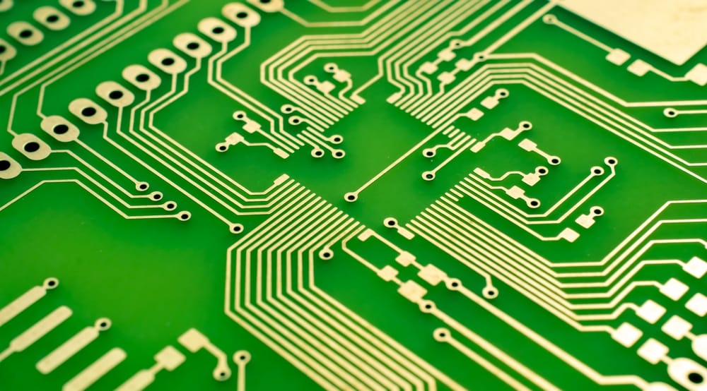
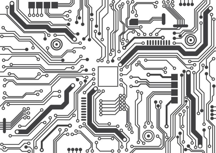
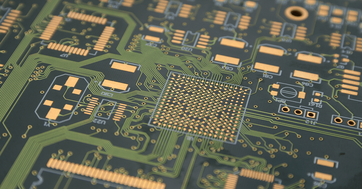
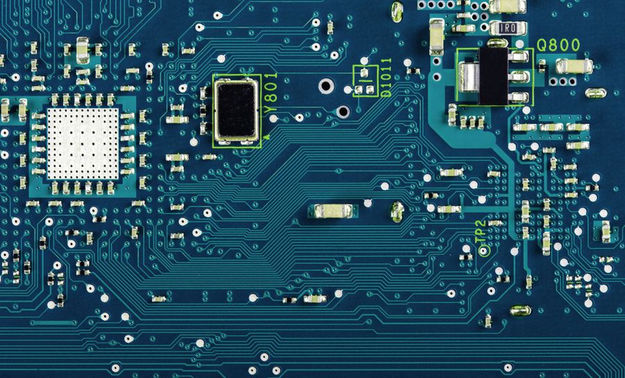
A PCB trace is a highly conductive track that is used to connect components on a printed circuit board. The traces are commonly made of copper and are fabricated during the etching process of a PCB. This article delves into the explanation of PCB trace, its vital components, and its significance to PCB design and fabrication.

The complete guide to PCB pad :types, size, spacing, repair and comparison - IBE Electronics

Understanding Double-Sided PCBs: A Comprehensive Guide
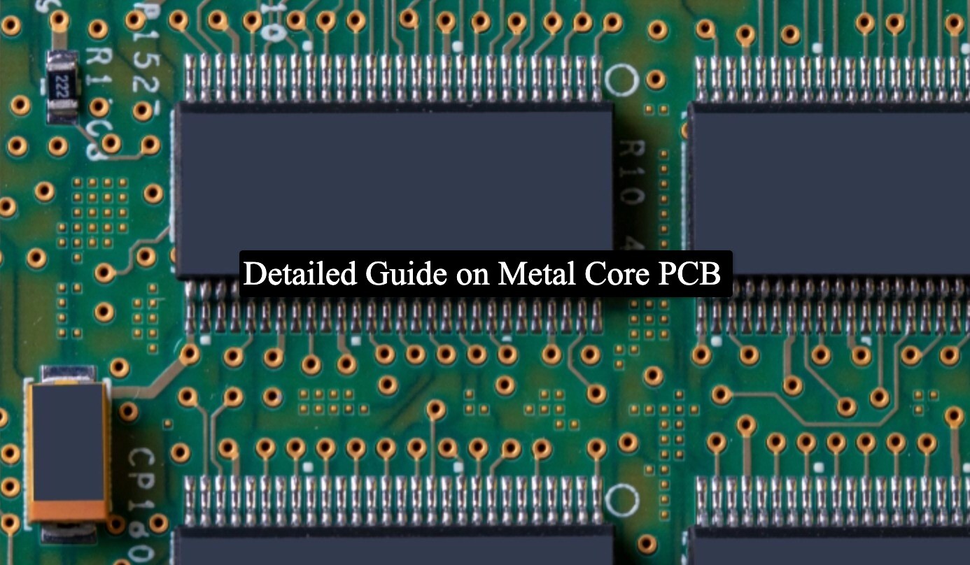
Detailed Guide on Metal Core PCB - Absolute Electronics Services
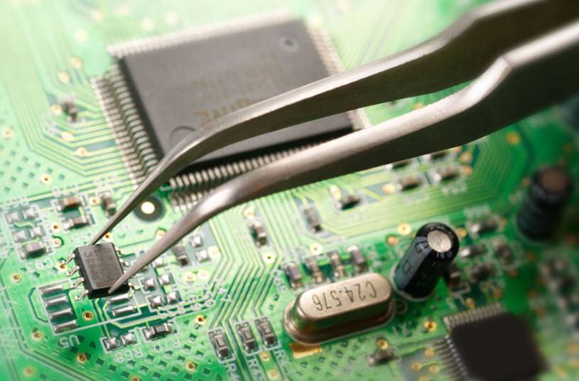
Ultimate Guide to Benchtop PCB Rework & Repair
PCB Colors -The Most Comprehensive Guide You need to know

Why can't PCB traces be too long? - IBE Electronics
What is a Via: A Comprehensive Guide
Trace PCB: A Comprehensive Guide

A complete guide on PCB copper trace - PCBA Manufacturers

The Comprehensive Guide to PCB Reverse Engineering

PCB Trace Width, Thickness, Spacing, and Length