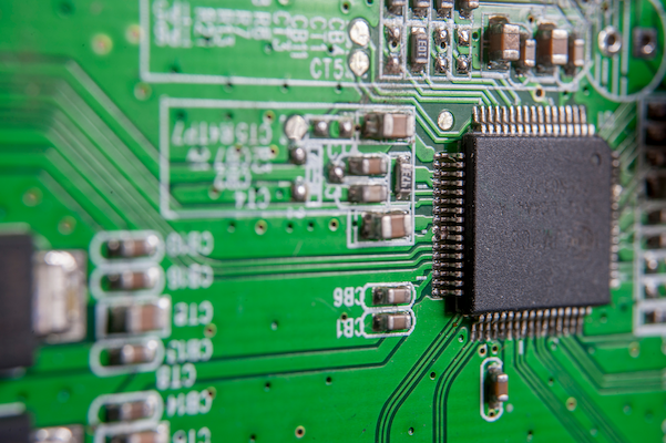
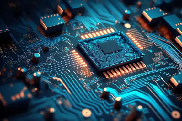
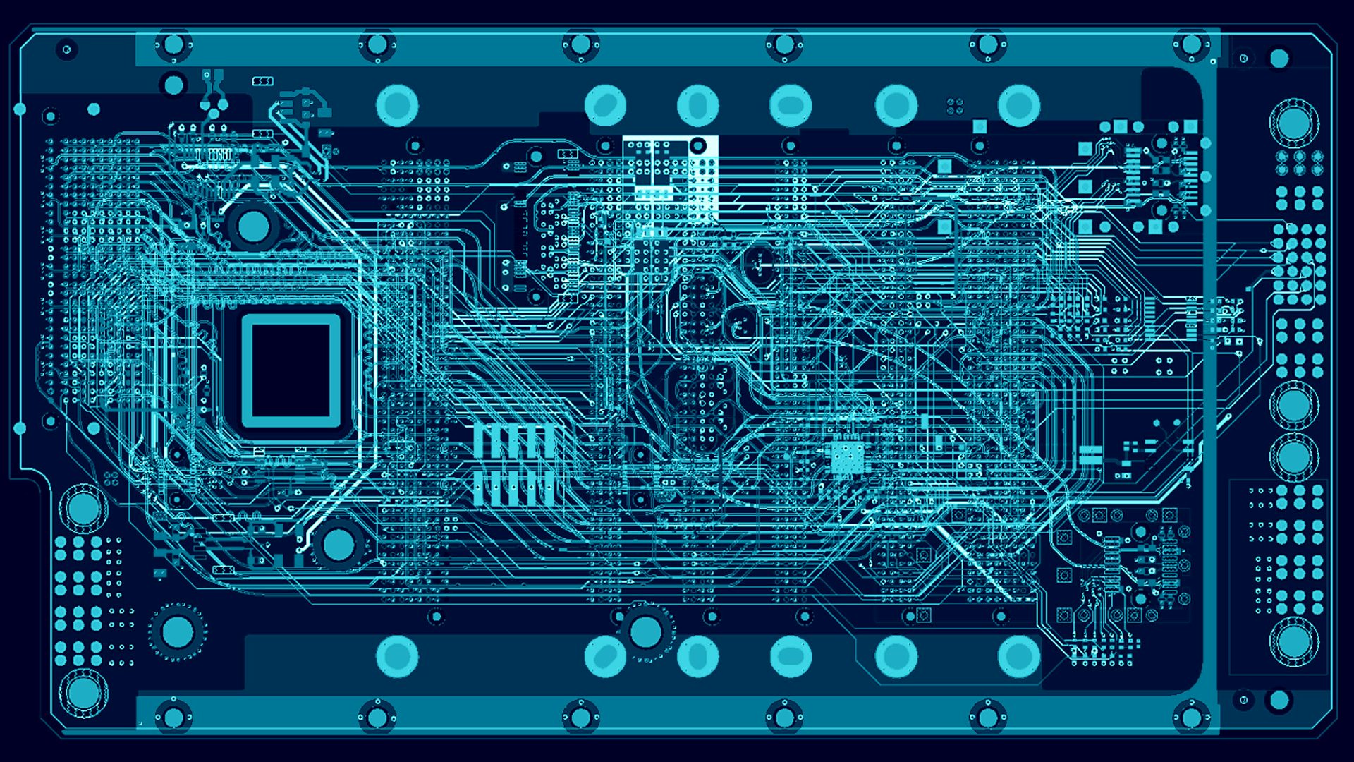
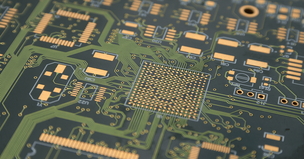
The printed circuit board design (also called PCB design) is based on the circuit schematic diagram to achieve the functions required by the circuit designer. PCB design mainly refers to the PCB layout design, and the layout of the external connection needs to be considered, and optimized layout of internal electronic components. Optimized layout of metal
What is Printed Circuit Board and Designing Process of PCB?

How to Design a PCB Layout - Circuit Basics

3 PCB Layout Principles for ESD Protection

PCB Design 101: The Basics of PCB Design - MorePCB

A detailed guide to PCB layout design - IBE Electronics
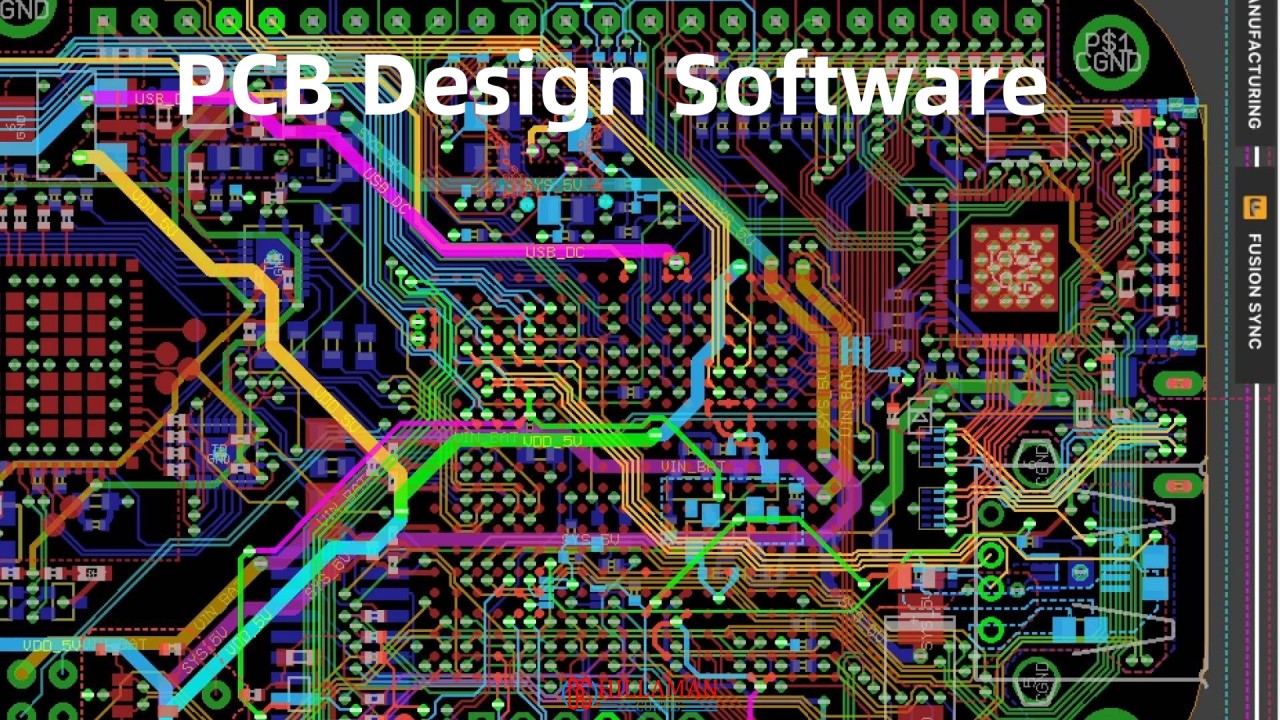
Best 8 Free Printed Circuit Board Design Software
High Performance PCB Systems Design and Analysis Guide, Advanced PCB Design Blog
Sensors and PCB design
How to Design a PCB Layout - Circuit Basics

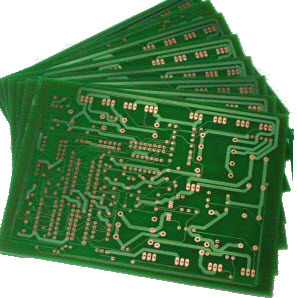
PCB Layout and Design Services - Printed Circuit Board Fabrication